- 您现在的位置:买卖IC网 > Sheet目录337 > LDS8868-002-T2 (IXYS)IC LED DVR WHT/CLR BCKLGT 16WQFN
LDS8868
1.5V), LDS8868 restores LED current at this
particular channel to programmed value.
2. V OUT Over-Voltage Protection
The charge pump’ output voltage V OUT automatically
limits at about 6.2 V maximum. This is to prevent the
output pin from exceeding its absolute maximum
rating.
3. V OUT Short Circuit Protection
If V OUT is shorted to ground before LDS8868 is
enabled, input current may increase up to 200 – 300
mA within 20 μs after enable and is limited to 35 – 40
mA after that.
4. Over-Temperature Protection
If the die temperature exceeds +150°C, the driver will
enter shutdown mode. The LDS8868 requires restart
after die temperature falls below 130°C.
5. Input Voltage Under-Voltage Lockout
If V IN falls below 2.2 V (typical value), LDS8868
enters shutdown mode and all registers data are
cleared. Device requires restart when input voltage
rises above 2.3 V. To restart device, set EN/SET pin
logic low, turn V IN off/on, set EN/SET pin logic high,
and program I LED using 1-wire interface.
6. Low V IN or High LED V F Voltage Detection
If, in 2x mode, V IN is too low to maintain regulated
LED current for given LED V F , or LED becomes an
open circuit, or if any LED at active channels is
In 1x mode, the device operates in linear mode and
does not introduce switching noise back onto the
supply.
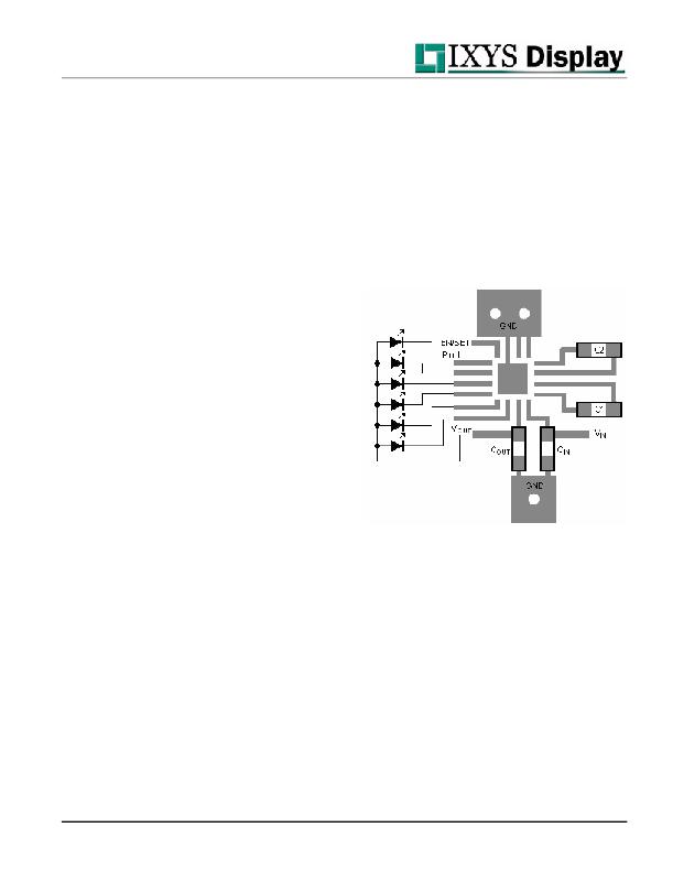
Recommended Layout
In charge pump mode, the driver switches internally
at a high frequency. It is recommended to minimize
trace length to all four capacitors. A ground plane
should cover the area under the driver IC as well as
the bypass capacitors. Short connection to ground on
capacitors C IN and C OUT can be implemented with the
use of multiple via. A copper area matching the
TQFN exposed pad (TAB) must be connected to the
ground plane underneath. The use of multiple via
improves the package heat dissipation.
disconnected,
LDS8868
starts subsequently
changing modes (2x – 1x –1.5x – 2x -…) in an
attempt to compensate insufficient voltage. As a
result, average current at all other channels that are
ON may fall below regulated level.
LED Selection
LEDs with forward voltages (V F ) ranging from 1.6 V to
3.6 V may be used. Charge pumps operate in highest
efficiency when V F voltage is close to V IN voltage
multiplied by switching mode, i.e. V IN x 1, V IN x 1.5,
and so on. If the power source is a Li-ion battery,
LEDs with VF = 2.7V - 3.3V are recommended to
achieve highest efficiency performance and extended
operation on a single battery charge.
External Components
The driver requires two external 1 μF ceramic capa-
citors (C IN and C OUT ) and two 0.22 μF ceramic capa-
citors (C1 and C2) X5R or X7R type. Capacitors C1
and C2 may be increased up to 1 μF to improve
charge pump efficiency by 3%. In all charge pump
modes, the input current ripple is very low, and an
input bypass capacitor of 1μF is sufficient.
Figure 4. Recommended layout
? 2009 IXYS Corp.
Characteristics subject to change without notice
11
Doc. No. 8868_DS, Rev. N2.1
发布紧急采购,3分钟左右您将得到回复。
相关PDF资料
LDS8869-002-T2
IC LED DVR WHT/CLR BCKLGT 16WQFN
LDV100-012SN
POWER SUPPLY LED 90W 12V COMPACT
LDV100-024SN
POWER SUPPLY LED 100W 24V COMPAC
LE25S40MB-AH
IC MEM 4MBIT SERIAL FLASH 8SOP
LE25U20AMB-AH
IC MEM 2MBIT SERIAL FLASH 8SOP
LFDAS12XSIT
HARDWARE MC9S12XS 112-PIN
LFXP10E-L-EV
BOARD EVAL LATTICEXP10E STD
LH28F008SCHT-TE
IC FLASH 8MBIT 85NS 40TSOP
相关代理商/技术参数
LDS8869-002-T2
功能描述:IC LED DVR WHT/CLR BCKLGT 16WQFN RoHS:是 类别:集成电路 (IC) >> PMIC - LED 驱动器 系列:PowerLite™ 标准包装:60 系列:- 恒定电流:- 恒定电压:- 拓扑:线性(LDO),PWM,升压(升压) 输出数:8 内部驱动器:是 类型 - 主要:背光 类型 - 次要:RGB,白色 LED 频率:500kHz ~ 1.5MHz 电源电压:4.75 V ~ 26 V 输出电压:45V 安装类型:* 封装/外壳:* 供应商设备封装:* 包装:* 工作温度:-40°C ~ 85°C
LDS9003-002-T2
功能描述:LED照明驱动器 High Power LED Temp & PWM Contr
RoHS:否 制造商:STMicroelectronics 输入电压:11.5 V to 23 V 工作频率: 最大电源电流:1.7 mA 输出电流: 最大工作温度: 安装风格:SMD/SMT 封装 / 箱体:SO-16N
LDS-A2802RI
功能描述:LED 显示器和配件 .28" Sng Digit Disp 565nm Green LEDs RoHS:否 制造商:Avago Technologies 显示器类型:7 Segment 数位数量:2 字符大小:7.8 mm x 14.22 mm 照明颜色:Red 波长:628 nm 共用管脚:Common Anode 工作电压:2.05 V 工作电流:20 mA 最大工作温度:+ 85 C 最小工作温度:- 35 C 封装:Tube
LDS-A2802RI-SUG
功能描述:LED 显示器和配件 .28" Sng Digit Disp 574nm Green LEDs RoHS:否 制造商:Avago Technologies 显示器类型:7 Segment 数位数量:2 字符大小:7.8 mm x 14.22 mm 照明颜色:Red 波长:628 nm 共用管脚:Common Anode 工作电压:2.05 V 工作电流:20 mA 最大工作温度:+ 85 C 最小工作温度:- 35 C 封装:Tube
LDS-A2804RI
功能描述:LED 显示器和配件 .28" Sng Digit Disp 635nm Red LEDs RoHS:否 制造商:Avago Technologies 显示器类型:7 Segment 数位数量:2 字符大小:7.8 mm x 14.22 mm 照明颜色:Red 波长:628 nm 共用管脚:Common Anode 工作电压:2.05 V 工作电流:20 mA 最大工作温度:+ 85 C 最小工作温度:- 35 C 封装:Tube
LDS-A2804RI-750
功能描述:LED 显示器和配件 LED Display RoHS:否 制造商:Avago Technologies 显示器类型:7 Segment 数位数量:2 字符大小:7.8 mm x 14.22 mm 照明颜色:Red 波长:628 nm 共用管脚:Common Anode 工作电压:2.05 V 工作电流:20 mA 最大工作温度:+ 85 C 最小工作温度:- 35 C 封装:Tube
LDS-A301BE
功能描述:LED 显示器和配件 LED Display RoHS:否 制造商:Avago Technologies 显示器类型:7 Segment 数位数量:2 字符大小:7.8 mm x 14.22 mm 照明颜色:Red 波长:628 nm 共用管脚:Common Anode 工作电压:2.05 V 工作电流:20 mA 最大工作温度:+ 85 C 最小工作温度:- 35 C 封装:Tube
LDS-A301BI
功能描述:LED 显示器和配件 LED Display RoHS:否 制造商:Avago Technologies 显示器类型:7 Segment 数位数量:2 字符大小:7.8 mm x 14.22 mm 照明颜色:Red 波长:628 nm 共用管脚:Common Anode 工作电压:2.05 V 工作电流:20 mA 最大工作温度:+ 85 C 最小工作温度:- 35 C 封装:Tube